"Put you left foot in, take your left foot out" Lab
| Explore latch and flipflop design | |
| Sequential circuit design |
| 7400 quad 2-input NAND gates | |
| 7402 quad 2-input NOR gates | |
| 7404 hex INVERTER gates | |
| 7475 4-bit D latch | |
| 7476 dual JK flipflops with preset/clear |
And others? Pinouts for these guys are attached.
Last lab went well. Just don't forget the basics:
| For your safety... unplug the logic box while you are working on it! | |
| For the health and safety of your chips... watch your power and ground inputs! |
This lab focuses on sequential circuit design, described in Chapter 6 of our text.
Build an SR latch out of NOR gates ala Figure 6-4 on page 245 of our text.
Draw your circuit diagram. Label inputs with switch #'s, outputs with LED #'s and NOR connections with pin numbers from the chip.
Complete this table:
S R Q Q' Description 0 0 1 0 0 0 0 1 0 0 1 1
Sorry. You can pull apart your old SR latch. We're now going to build one with NAND gates, and a control input. The circuit diagram is Figure 6-7 on page 247 of our text.
Please use one of the pulse buttons for the control input to mimic a clock input. For example, use PB1 (_/ \_) for a pulse that goes high (to logic 1) when you press the PB button.
Again, show your circuit diagram, properly labeled, and complete the table below:
C S R Q Q' Description 0 0 0 0 1 0 0 0 0 0 0 1 1 0 0 1 0 1 1 0 0 1 1 0 1 0 0 1 1 1 Note: Don't disassemble this circuit!!!
Next to your SR latch with control, please connect the 7475 D latch. Again, you can use a PB as input.
Fill out the table:
C D Q Q' Description 0 0 0 1 1 0 1 1 Note: Do not disassemble this circuit, read on...
Using your D latch and your SR latch with control and a few inverters ala Figure 6-13 on page 253 of our text, build a positive-edge-triggered D flipflop.
Fill out a table exercising your flipflop's function.
If you do this one, please show it to me.
Choose one of the two problems below and implement it with JK flipflops and whatever logic you deem necessary:
Design a sequential circuit (using JK flipflops) that satisfies the following state table:
Present State
Input Next State
Output A B X A B Y 0 0 0 0 0 0 0 0 1 0 1 0 0 1 0 0 0 1 0 1 1 1 1 0 1 0 0 0 0 1 1 0 1 1 0 0 1 1 0 0 0 1 1 1 1 1 0 0 Please draw your state diagram, your logic design work to get minimized flipflop equations, your circuit diagram (with switches, pins, etc labeled) and show me your result once it's working.
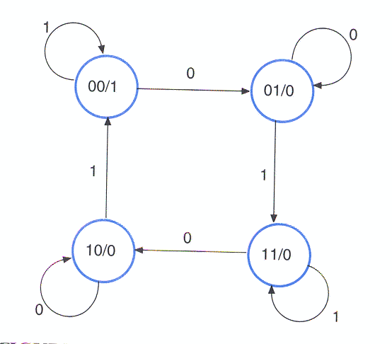
Design a sequential circuit (using JK flipflops) that satisfies the following state diagram:
Please draw your state diagram, your logic design work to get minimized flipflop equations, your circuit diagram (with switches, pins, etc labeled) and show me your result once it's working.
Do your usual report... let me see your masterpiece when it's ready.